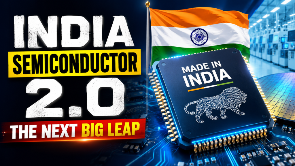
Make in India Semiconductor 2.0: The Next Big Leap for Chip Manufacturing
By Kaushik Brahmakshatriya
Published On 04 July 2026.
India Semiconductor Mission 2.0
India’s dream of becoming a global semiconductor powerhouse just got a massive boost. The Union government has cleared an outlay of nearly ₹1.25 lakh crore for the second phase of the India Semiconductor Mission, widely known as ISM 2.0. This marks one of the biggest financial commitments yet under the broader Make in India push, and it signals that the country is moving beyond assembly work into deeper, more strategic areas of chip design and manufacturing
The first phase of the mission, launched in 2021 with a ₹76,000 crore budget, laid the groundwork. It brought in fabrication units, packaging plants, and design incentives that helped India attract global players. ISM 2.0 builds on that foundation with a sharper focus on equipment, raw materials, intellectual property, and research infrastructure.
Why ISM 2.0 Matters
Chips power almost everything today, from smartphones and cars to defence systems and AI infrastructure. India currently imports the bulk of its semiconductor needs, so building domestic capacity isn’t just an economic goal, it’s a matter of long-term technological independence. ISM 2.0 is designed to reduce that dependence while positioning India as a trusted alternative in the global supply chain.
Key Highlights of ISM 2.0
| Aspect | ISM 1.0 (2021) | ISM 2.0 (2026) |
| Total Outlay | ₹76,000 crore | ₹1.25 lakh crore (approx.) |
| Focus Areas | Fabs, ATMP/OSAT, Design (DLI) | Equipment, materials, IP, R&D centres |
| Projects Approved | 10-13 major units | Expanded pipeline expected |
| Fiscal Support | Up to 50% of project cost | Continued, with added incentives |
Projects Approved Under the Mission So Far
| Project Type | Example / Location | Status |
| Semiconductor Fab | Tata Semiconductor Manufacturing | Approved |
| ATMP/OSAT Plant | Micron Technology, Sanand, Gujarat | Operational |
| Compound Semiconductor Fab | CG Power & CG SEMI | Approved |
| Display Manufacturing | GaN-based mini/micro-LED unit | Approved |
| Packaging & Testing | Kaynes Semicon, Sanand, Gujarat | Operational |
What Comes Next
With the Expenditure Finance Committee clearing the outlay, the proposal now moves to the Union Cabinet for final approval. Once cleared, ISM 2.0 is expected to accelerate work on advanced technology nodes, expand the domestic design ecosystem, and build a skilled workforce through dedicated research and training centres. Industry watchers believe India’s semiconductor market could touch $100-110 billion by 2030, making this a defining decade for the sector.
Frequently Asked Questions
Q1: What is India Semiconductor Mission 2.0?
It is the second phase of India’s flagship semiconductor programme, focused on strengthening chip design, manufacturing, materials, and research capabilities with a significantly larger budget than the first phase.
Q2: How much money has been allocated to ISM 2.0?
The government has cleared an outlay of approximately ₹1.25 lakh crore, though final approval from the Union Cabinet is still pending.
Q3: How is ISM 2.0 different from ISM 1.0?
While ISM 1.0 focused mainly on setting up fabs and packaging units, ISM 2.0 places greater emphasis on equipment, raw materials, indigenous chip design IP, and R&D infrastructure.
Q4: Which companies are involved in India’s semiconductor push?
Major players include Tata Electronics, Micron Technology, CG Power, and Kaynes Semicon, among others operating fabs and packaging units across states like Gujarat.
Q5: What is the long-term goal of the mission?
India aims to build a self-reliant, full-stack semiconductor ecosystem covering design, fabrication, and packaging, reducing import dependence and supporting sectors like AI, defence, and telecom.
Disclaimer: This article is for informational purposes only and reflects publicly available government updates as of early July 2026. Readers should verify final Cabinet approvals through official sources before citing figures.